Samsung Electro-Mechanics and Sumitomo Chemical Bet on ‘Glass Core’ for Substrate Race
Published: 11.13.2025
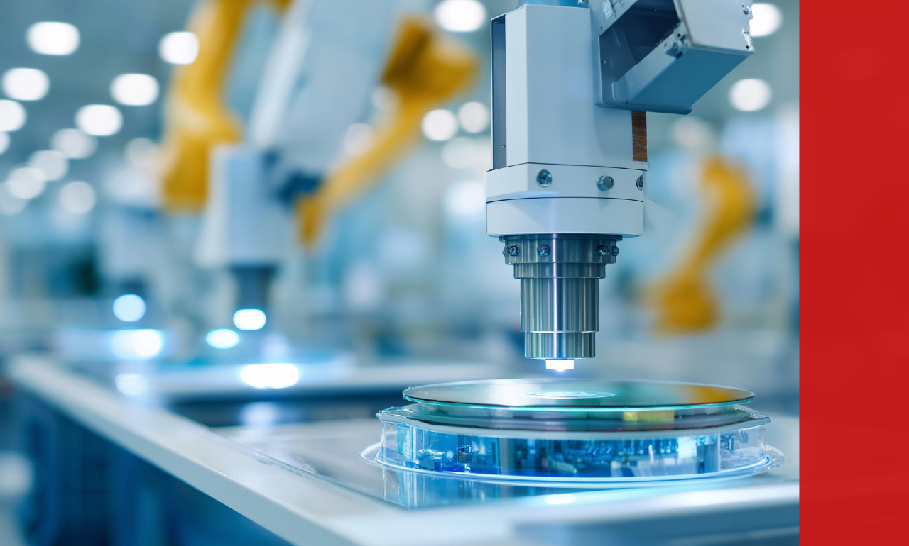
- Samsung Electro-Mechanics has signed an MOU with Japan’s Sumitomo Chemical Group to establish a joint venture focused on “Glass Core” base materials for next-generation glass package substrates.
- Glass substrates can boost data transmission speeds by up to 40% and reduce power consumption by around 30% compared to traditional PCB materials.
- The global glass substrate market is projected to reach US$198 million by 2025, growing at a CAGR of 15.9% through 2033, driven by AI, data centers, and 5G/6G infrastructure.
Samsung Electro-Mechanics has signed an MOU with Japan’s Sumitomo Chemical Group to create a joint venture dedicated to manufacturing “Glass Core” as the base material for next-generation glass package substrates.
According to Samsung, the MOU signing ceremony took place in Tokyo on November 4, attended by SEMCO president Chang Duckhyun, Sumitomo Chemical chairman Keiichi Iwata, president Nobuaki Mito, and Lee Jongchan, president of Sumitomo subsidiary Dongwoo Fine-Chem
Industry coverage adds that Samsung Electro-Mechanics has already built a pilot line for glass substrates at its Sejong facility, is supplying sample glass package substrates, and is targeting mass production around 2027 and beyond, with the JV expected to be central to that ramp.
Why “Glass Core” matters for AI and high-performance computing
In its announcement, Samsung highlights Glass Core as an “essential technology” for high-density, large-area advanced package substrates, thanks to lower coefficient of thermal expansion and superior flatness compared with conventional organic cores.
As AI accelerators and HPC devices grow in size and complexity, current organic substrates struggle with warpage, limited routing density, and power delivery constraints. Intel’s own glass-substrate R&D, for example, points to much higher interconnect density, ultra-low warpage, and better mechanical/thermal stability, enabling more powerful data-center and AI packages later this decade.
The IC-PCB analysis of the Samsung–Sumitomo move notes that glass substrates can improve data transmission speeds by up to about 40% and reduce power consumption by roughly 30% versus traditional organic PCB substrates that speak directly to AI server and GPU power-performance trade-offs.
Meanwhile, a recent deep-dive on glass core substrates and interposers based on Yole Group’s “Glass Materials for Advanced Packaging 2025” report argues that glass has moved from carrier roles into a central enabling material for chiplet fabrics, co-packaged optics, and RF front-ends in data centers and 5G/6G telecom.
Glass substrates set for double-digit growth
Market-research firm Data Insights Market estimates that the global market for glass substrates used in advanced packaging will reach about US$198 million in 2025, with a projected CAGR of roughly 15.9% from 2025 to 2033, driven primarily by data-center and AI workloads, along with 5G infrastructure and high-performance electronics.
The same report lists AGC, Schott, and Corning among key glass players, and highlights that glass substrates are increasingly used in high-density interconnects and 3D stacking for advanced packaging.
Layered on top of that, the Yole characterizes glass materials as entering a “high-growth phase,” with regional ecosystems in China, Korea, and Japan rapidly building capacity to support local AI/HPC and telecom demand.
Within this landscape, Samsung Electro-Mechanics is positioning itself as a front-runner in glass substrate commercialization, already supplying sample glass substrates to select customers and targeting volume production around 2027, according to IC-PCB and Korean media coverage.


