Lam Research and CEA-Leti Expand R&D to Fast-Track Multi-Element Materials for Specialty Semiconductors
Published: 2.13.2026
- Lam Research and CEA-Leti signed a multi-year R&D agreement to explore novel multi-elemental materials and process pathfinding for higher-efficiency compound semiconductors and next-gen Specialty Technology devices.
- The scope spans MEMS, 3D imaging/sensors, power management, RF, photonics (including MicroLED), and optical interconnect the “system enablers” increasingly limiting AI-era performance.
- A key goal is to bridge lab results to manufacturing readiness, with CEA-Leti describing an ambition to reach TRL 6
The next semiconductor breakthrough may not come from smaller transistors but from new materials.
On February 2, 2026, Lam Research and CEA-Leti have signed a multi-year research agreement aimed at accelerating multi-element materials development and advancing manufacturing-ready processes for next-generation specialty semiconductors. The collaboration focuses on enabling higher-efficiency compound semiconductor devices used in AI infrastructure, RF systems, silicon photonics, power management, and optical interconnect technologies.
As AI workloads scale and high-performance computing systems push energy and bandwidth limits, traditional silicon scaling is no longer the only driver of performance. The industry is now confronting system-level bottlenecks in power delivery, thermal management, data movement, and RF efficiency, all areas where advanced materials are becoming critical.
Why Multi-Element Materials Matter for AI Infrastructure
Under the deal, the partners will explore novel multi-elemental materials and pathfinding for future fabrication processes aimed at higher-efficiency compound semiconductors with the work positioned for AI and high-performance computing needs.
EE Times reported the agreement was signed on Jan. 30, 2026 in Grenoble, France, and that it builds on an existing collaboration, particularly around plasma-based process technologies.
Lam’s own framing is specialty technologies are increasingly essential for AI infrastructure because power and connectivity bottlenecks can cap overall system performance. In that view, innovations in power electronics and silicon photonics are becoming central to AI-era roadmaps, not side quests.
This is why the partnership’s target list matters. Optical interconnect and photonics speak directly to the data-movement problem. Power management speaks to energy efficiency and thermal limits. Sensing and imaging tie into expanding AI beyond the data center into physical systems and industrial environments.
The Technical Bet on Multi-Element Materials
As EE Times explains, compound and multi-element materials are increasingly relevant for RF components, power electronics, photonics, and optical interconnect, where they can enable improvements like higher switching speed, better signal integrity, and more efficient power conversion. But those same materials also introduce major manufacturing complexity, raising the premium on tight coordination between equipment capability and process integration.
One of the clearest “industry voice” comments came from Chris Carter, group VP and GM at Lam’s Customer Support Business Group, who told EE Times that new semiconductor materials can break traditional tradeoffs and deliver “step-function improvements.”
That’s the bet: materials innovation that moves the needle on performance-per-watt. The risk: integration, repeatability, and manufacturability.
How Lam and CEA-Leti Split the Work
The logic of the partnership is complementary capability:
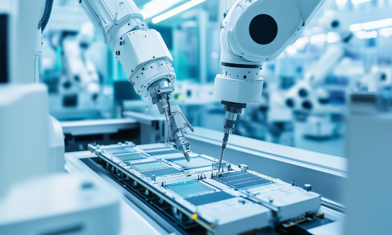
- Lam Research brings advanced etch and deposition platforms to develop and tune new films and structures. The company highlights that its process capabilities, alongside deposition approaches such as pulsed laser deposition (PLD), will be used in the research.
- CEA-Leti brings deep materials analysis, metrology, and device characterization, enabling rapid feedback on how process changes affect material properties and device performance.
Lam CTO Vahid Vahedi framed the agreement around speed-to-impact: the collaboration will combine Lam’s etch/deposition strengths with CEA-Leti’s characterization expertise to “fast-track” more energy-efficient, higher-performance specialty devices.
CEA-Leti CEO Sébastian Dauvé emphasized the mechanism: rapidly characterizing how materials behave in complex device structures to pinpoint integration challenges and provide “actionable feedback,” accelerating the move from promising process innovation to validated functionality and industrialization readiness.
Dauvé told EE Times that CEA-Leti often operates at TRL 4–5, but here the objective is to reach TRL 6, which he described as a “gateway to industrialization.”
EE Times also highlighted a practical reason industrial partners care: when a research institute works alone, questions arise about portability and scalability, but co-developing with a “reference research institute” can reduce perceived risk for manufacturing adoption.
Where the Work is Pointed First
The core focus of this collaboration is on multi-elemental (compound) materials including:
- RF filters and front-end modules
- Power electronics and advanced power management
- Silicon photonics and optical interconnect
- Electro-optic modulation
- MicroLED and advanced display technologies
- Emerging quantum photonics applications
EE Times adds additional context from Dauvé on why photonics is a timely anchor point: “Photonics for data communications in data centers” is a clear example driving demand for new materials and advanced deposition/etching processes, alongside integration of new photonic materials and packaging technologies.


